I currently need a high power 12V power supply (to feed a Class-D amp, which in turn is going to provide an easily tuned source of ~60Hz power, to drive a stirling cycle helium cryocooler, to make liquid nitrogen - more on that another time).
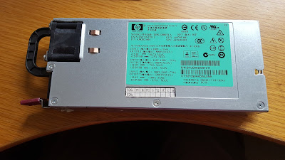
Lots of people in the RC community have hacked server power supplies to this purpose, and I happen to have a couple of HP 1200W DL580 PSUs to hand which should both be fairly easy to adapt, and offer pretty high efficiency.
![]()
Looking on the various blogs, the current most common way to get these supplies to operate, is by attaching an ~1K resistor between pins 33 & 36 http://www.rchelination.com/setting-hp-dps-1200fb-power-supply/ , but there are very few details as to why this works.
As part of my "day job" I've worked on the design of quite a few systems using high power PSUs, and I was keen to understand a bit more about these units before just hacking away. I also wanted to see if there was a way to easily monitor the output voltage and current of the supply from a Raspberry Pi (most PSU of this class have an I2C bus).
The DL580 1200W PSU is just one of a range of HP PSUs which fit into servers with the "Common Slot" support http://www.hp.com/ctg/Manual/c03502743.pdf .
Compatible units have varying powers and efficiencies, but all share the same physical form factors, which has power entry at the front (DC or AC)
![]()
and an edge connector at the back which feeds power to the server and provides control & monitoring.
![]()
That the two large areas provide the main 12V feed is both obvious and well proven, but I couldn't easily find any details on the control signals (contacts 27-38).
Having designed with similar supplies in the past I've got a fairly clear idea of the kind of signals which should be the interface: present, enable, PMBUS serial interface (address setting, SCL/SDA & alarm), standby power, current share, possibly remote sense, etc) but I wanted to have precise details.
Some quick work with the multimeter, a peek at the PCB, some prior knowledge of similar units, and a bit of I2C bus analysis suggests the following assignments for the bottom contacts:
27-29 = Used at start of day to set PMBus slave address for the PSU (at least I've verified 27 causes an address change, and I suspect the other two will also).
30 = Signal Gnd
31 & 32 = PMBus SDA/SCL lines allowing monitoring and control of the PSU inline with https://en.wikipedia.org/wiki/Power_Management_Bus (This is something I plan to explore further in the future)
Looking at the top:
38 = PS alarm
I know that PMBus PSUs normally have an active low alarm output, and from the idle voltages and unpowered resistance, I am fairly certain that this is pin 38
37 = 12V Standby Power
Good for 2.5A, and perfect for powering a 12V-5V converter for the Raspberry Pi I want to use for monitoring/control.
That leaves 33,34,35 & 36.
33 & 36 are clearly involved in enabling the supply, both because that is where people are currently connecting a resistor, and because 36 is a short "last make / first break" contact. Having said that, I wasn't convinced that the intended mode of operation was to join the two signals with a resistor.
I have various reasons for this belief, including that:
36 = Present
Having taken some measurement on a live server, I am fairly certain that 36 is a dual purpose "present" signal which is pulled up by the platform from a voltage derived from the standby power. When a PSU slot is empty (but the server has other PSUs in place), this signal will be high on the server side showing no PSU in place. When a PSU is inserted, the server signal is clamped to about 0.53V (a typical diode drop, or transistor base voltage) by the PSU which allows the server to notice a new PSU. From the PSU perspective, this input being pulled up tells the PSU that it is full inserted (making the transistor base interpretation more likely).
In my testing, a 22K resistor between pin 36 & 12V Standby power (pin 37) is enough to make the PSU think it is inserted into a slot. With the clamp action of the input, this gives around 500uA of current.
33 = Enable#
With the Present pin biased from 12VSB, pulling pin 33 directly to ground causes the main 12V output to enable. Looking at the current, open voltage and operation point, it looks like the pin is pulled up to the PSU internal 3V3 bus via a 10K resistor, and is monitored via a standard CMOS Schmitt trigger input gate.
I've not yet tried controlling the PSU over the PMBus, but PSU of this type can typically be enabled either via the Enable# pin, or via software control.
This splitting of 33 & 36, into a pulled up / clamped "present" signal, and a simple pull to ground "enable#" signal (which can also be driven over I2C) is much more consistent with other PSU I have worked with.
Given this understanding, you can see why the resistor between 33 & 36 works, because you are using the pull up on the Enable# input to bias the Present signal, and that load is in turn pulling Enable# low enough to operate.re is a fairly tight range of viable
However, in my own supply I will simply be going with a fixed 22K resistor from Present to 12VSB, and a separate switch between Gnd and Enable#, as that leaves the possibility of software control over the PMBus.
That now leaves two pins, 34 & 35.
34 = Current Monitor
Based on some testing I think 34 is a current monitor output. I've only tested low currents so far, but I think the output is around 60mV/A. I'll update this figure once I've tested to full range. If I can't get the PMBus interface to work, this analog signal will still provide a useful means of monitoring current draw, A 6:1 resistive divider to ground would give 10mV/A, and you could then connect a cheap 0-1V voltmeter module, ideally with programmable decimal place, to directly display current in A.
35 = PSU status
That leaves 35 as the last pin, and I think it is a PSU status pin, providing a similar indication to the front panel LED. I'm guessing that it will be multi-level to allow error indications, but don't yet have a clear mapping, except to say that this pin shows 0V09 when the PSU is plugged in, but not enabled, and 3V2 then the PSU is enabled.
In terms of current sharing between loads, I'm fairly sure that it is simple "Active Droop", of around 3mV/A.
I am surprised not to see remote voltage sensing (to allow compensation for connector voltage drop), but given the above assignments there are no obviously spare pins for this function. I have seen in the past PMBus address setting done via an analog input & resistor value, so if it was going to be anywhere, then I'd look at pins 28 & 29. Something to explore further next time I remove the PCB from the case.
Finally, I've done some research and believe the matching socket (vertical variant) for the edge connector is FCI part 10046971-001LF which is available from a number of places including Digikey and Mouser. I have a couple on order and will report back if they fit properly. If they do, this will mean I can solder the load wires to the connector and simply plug in the unaltered PSU.
Lots of people in the RC community have hacked server power supplies to this purpose, and I happen to have a couple of HP 1200W DL580 PSUs to hand which should both be fairly easy to adapt, and offer pretty high efficiency.
Looking on the various blogs, the current most common way to get these supplies to operate, is by attaching an ~1K resistor between pins 33 & 36 http://www.rchelination.com/setting-hp-dps-1200fb-power-supply/ , but there are very few details as to why this works.
As part of my "day job" I've worked on the design of quite a few systems using high power PSUs, and I was keen to understand a bit more about these units before just hacking away. I also wanted to see if there was a way to easily monitor the output voltage and current of the supply from a Raspberry Pi (most PSU of this class have an I2C bus).
The DL580 1200W PSU is just one of a range of HP PSUs which fit into servers with the "Common Slot" support http://www.hp.com/ctg/Manual/c03502743.pdf .
Compatible units have varying powers and efficiencies, but all share the same physical form factors, which has power entry at the front (DC or AC)

and an edge connector at the back which feeds power to the server and provides control & monitoring.

That the two large areas provide the main 12V feed is both obvious and well proven, but I couldn't easily find any details on the control signals (contacts 27-38).
Having designed with similar supplies in the past I've got a fairly clear idea of the kind of signals which should be the interface: present, enable, PMBUS serial interface (address setting, SCL/SDA & alarm), standby power, current share, possibly remote sense, etc) but I wanted to have precise details.
Some quick work with the multimeter, a peek at the PCB, some prior knowledge of similar units, and a bit of I2C bus analysis suggests the following assignments for the bottom contacts:
27-29 = Used at start of day to set PMBus slave address for the PSU (at least I've verified 27 causes an address change, and I suspect the other two will also).
30 = Signal Gnd
31 & 32 = PMBus SDA/SCL lines allowing monitoring and control of the PSU inline with https://en.wikipedia.org/wiki/Power_Management_Bus (This is something I plan to explore further in the future)
Looking at the top:
38 = PS alarm
I know that PMBus PSUs normally have an active low alarm output, and from the idle voltages and unpowered resistance, I am fairly certain that this is pin 38
37 = 12V Standby Power
Good for 2.5A, and perfect for powering a 12V-5V converter for the Raspberry Pi I want to use for monitoring/control.
That leaves 33,34,35 & 36.
33 & 36 are clearly involved in enabling the supply, both because that is where people are currently connecting a resistor, and because 36 is a short "last make / first break" contact. Having said that, I wasn't convinced that the intended mode of operation was to join the two signals with a resistor.
I have various reasons for this belief, including that:
- it is normal to have separate "enable"& "present" signals
- testing shows power up with a bridging resistor only works for quite a limited range of values, with resulting pin voltages which are quite atypical of these interfaces
- the voltage on pin 36 with the resistor present is very suggestive of a diode clamp to ground.
36 = Present
Having taken some measurement on a live server, I am fairly certain that 36 is a dual purpose "present" signal which is pulled up by the platform from a voltage derived from the standby power. When a PSU slot is empty (but the server has other PSUs in place), this signal will be high on the server side showing no PSU in place. When a PSU is inserted, the server signal is clamped to about 0.53V (a typical diode drop, or transistor base voltage) by the PSU which allows the server to notice a new PSU. From the PSU perspective, this input being pulled up tells the PSU that it is full inserted (making the transistor base interpretation more likely).
In my testing, a 22K resistor between pin 36 & 12V Standby power (pin 37) is enough to make the PSU think it is inserted into a slot. With the clamp action of the input, this gives around 500uA of current.
33 = Enable#
With the Present pin biased from 12VSB, pulling pin 33 directly to ground causes the main 12V output to enable. Looking at the current, open voltage and operation point, it looks like the pin is pulled up to the PSU internal 3V3 bus via a 10K resistor, and is monitored via a standard CMOS Schmitt trigger input gate.
I've not yet tried controlling the PSU over the PMBus, but PSU of this type can typically be enabled either via the Enable# pin, or via software control.
This splitting of 33 & 36, into a pulled up / clamped "present" signal, and a simple pull to ground "enable#" signal (which can also be driven over I2C) is much more consistent with other PSU I have worked with.
Given this understanding, you can see why the resistor between 33 & 36 works, because you are using the pull up on the Enable# input to bias the Present signal, and that load is in turn pulling Enable# low enough to operate.re is a fairly tight range of viable
However, in my own supply I will simply be going with a fixed 22K resistor from Present to 12VSB, and a separate switch between Gnd and Enable#, as that leaves the possibility of software control over the PMBus.
That now leaves two pins, 34 & 35.
34 = Current Monitor
Based on some testing I think 34 is a current monitor output. I've only tested low currents so far, but I think the output is around 60mV/A. I'll update this figure once I've tested to full range. If I can't get the PMBus interface to work, this analog signal will still provide a useful means of monitoring current draw, A 6:1 resistive divider to ground would give 10mV/A, and you could then connect a cheap 0-1V voltmeter module, ideally with programmable decimal place, to directly display current in A.
35 = PSU status
That leaves 35 as the last pin, and I think it is a PSU status pin, providing a similar indication to the front panel LED. I'm guessing that it will be multi-level to allow error indications, but don't yet have a clear mapping, except to say that this pin shows 0V09 when the PSU is plugged in, but not enabled, and 3V2 then the PSU is enabled.
In terms of current sharing between loads, I'm fairly sure that it is simple "Active Droop", of around 3mV/A.
I am surprised not to see remote voltage sensing (to allow compensation for connector voltage drop), but given the above assignments there are no obviously spare pins for this function. I have seen in the past PMBus address setting done via an analog input & resistor value, so if it was going to be anywhere, then I'd look at pins 28 & 29. Something to explore further next time I remove the PCB from the case.
Finally, I've done some research and believe the matching socket (vertical variant) for the edge connector is FCI part 10046971-001LF which is available from a number of places including Digikey and Mouser. I have a couple on order and will report back if they fit properly. If they do, this will mean I can solder the load wires to the connector and simply plug in the unaltered PSU.